Home / News / Industry News / What Is Precision Injection Molding? Electronic Precision Injection Molds, Scientific Injection Molding for Electronics, Explained
Industry News
Home / News / Industry News / What Is Precision Injection Molding? Electronic Precision Injection Molds, Scientific Injection Molding for Electronics, Explained
What is precision injection molding? Precision injection molding is an injection molding process in which every variable — melt temperature, injection speed, pack pressure, cooling time, and mold steel tolerance — is held to tighter specifications than conventional molding, producing parts with dimensional repeatability of ±0.01 to ±0.05 mm, gate vestige heights measured in micrometres, and surface finishes that meet SPI A1 or VDI 3400 texture standards without secondary operations. Electronic Precision Injection Molds are tooling sets built specifically to produce electronic housings, connector bodies, switch frames, sensor covers, and structural electronics components to the dimensional and surface quality standards that electronic assembly requires. Scientific injection molding is a data-driven methodology that uses Design of Experiments (DOE) and systematic process characterisation to establish a robust, documented molding process window that is independent of machine variation and operator interpretation. Scientific injection molding for electronics applies this methodology specifically to the tight-tolerance, high-reliability demands of the electronics sector, where a connector pin that is 0.1 mm out of position can prevent a PCB from seating. Precision injection molded electronics enclosures are the finished housings, shells, and frames produced by this combination of precision tooling and scientific process control, found in everything from handheld consumer devices to industrial control panels and medical monitoring equipment.
This guide explains how each concept works in practice, why standard injection molding cannot achieve the same results, and what engineering and tooling decisions determine whether a precision electronics enclosure program succeeds or requires costly rework.
Precision Injection Molding at a Glance
By Tolerance Class
Standard molding: ±0.1 to ±0.3 mm
Precision molding: ±0.02 to ±0.05 mm
Ultra-precision: ±0.005 to ±0.01 mm
Micro-molding: sub-micrometre features
By Process Approach
Conventional (operator-tuned)
Scientific injection molding (DOE-based)
Insert molding (electronics contacts)
Micro-molding (sub-1 gram shot weight)
By Electronics Application
Connector and terminal housings
Enclosures and EMI shield frames
PCB standoffs and alignment features
Sensor covers and optical windows
By Mold Steel Grade
P20: prototype or low volume
H13 hardened: standard precision
S136 stainless: optical or corrosive
NAK80: mirror-polish enclosures
What Is Precision Injection Molding? How It Differs from Standard Molding
Standard injection molding produces dimensionally acceptable parts by setting approximate process parameters and relying on experienced operators to adjust pressure, speed, and temperature until shots look acceptable. What is precision injection molding? It is the disciplined alternative: every parameter is characterised through systematic testing before production begins, and the resulting process window is documented, validated, and locked so that parts produced on Day 1 are dimensionally identical to parts produced 500,000 cycles later on a different shift. The tolerance standards that define precision molding in practice are approximately one order of magnitude tighter than standard production molding across every critical dimension.
±0.01 mm
Dimensional repeatability achievable with precision tooling and scientific process control
Cpk > 1.67
Process capability index target for critical dimensions in precision electronics molding programs
SPI A1
Highest optical surface finish grade, achievable with NAK80 or S136 mirror-polished cavities
0.05 mm
Typical maximum gate vestige height specification for precision injection molded electronics enclosures
Dimensional Tolerance Range by Molding Type (mm, lower = tighter)
The Four Variables That Separate Precision from Standard Molding
Precision injection molding differs from conventional molding in four fundamental areas, each of which must be addressed simultaneously to achieve the required dimensional performance:
Mold steel tolerance and surface condition: A precision injection mold for electronics is machined to cavity dimensional tolerances of ±0.005 to ±0.010 mm on critical features, using CNC machining centres with positional accuracy better than 0.002 mm and measured on CMM (coordinate measuring machine) after machining. The cavity surface is finished to the target texture specification with controlled polishing or EDM (electrical discharge machining) with verified surface roughness (Ra) values before the first test shot is made.
Machine capability and closed-loop process control: A precision molding machine monitors injection velocity, screw position, cavity pressure, and melt temperature on every shot and compares the values to the documented process window. Deviations exceeding a set tolerance trigger automatic shot rejection before the part is even ejected, preventing out-of-tolerance parts from entering the production stream. Machines used for precision injection molds programs typically have injection speed repeatability of better than 0.1% and screw position repeatability of 0.01 mm or better.
Resin lot qualification and drying: The same resin formulation from different production lots can vary in melt flow index (MFI) by ±10 to ±20%, which changes the viscosity of the melt and therefore the fill pressure, pack time, and final part dimensions. Precision programs qualify each incoming resin lot against the material specification, and critical moisture-sensitive engineering resins (PC, nylon, PBT) are dried to below 0.02% moisture by weight before processing to prevent hydrolytic degradation that changes viscosity and reduces mechanical properties.
Cooling system design and temperature control: In a precision injection mold, coolant temperature is controlled to ±0.5 degrees Celsius using temperature-controlled water units rather than plant cooling water, and the cooling circuit is designed to maintain uniform mold surface temperature across the cavity within ±2 degrees Celsius. A mold surface temperature variation of 5 degrees Celsius can produce a dimensional variation of 0.03 to 0.08 mm in a polycarbonate enclosure, which is larger than the allowable tolerance on many critical features.
Resin Selection for Precision Electronics Molding: What Changes at Tight Tolerances
The resin used in a precision injection molding program determines the mold's steel dimensions, cooling requirements, gate design, and process window. Every resin has a characteristic shrinkage range, and for Electronic Precision Injection Molds, the resin must have a predictable, narrow shrinkage range to allow the mold cavity to be cut to the correct dimension at first attempt:
Mold Shrinkage Range by Resin Type (%) — Narrower Range = More Predictable Dimensions
Common engineering resins used in precision injection molding for electronics, with their shrinkage ranges and key property trade-offs for enclosure applications
Resin
Mold Shrinkage
Key Strength
Key Limitation
Typical Electronics Use
PC (Polycarbonate)
0.5 to 0.7%
Optical clarity, impact resistance
Moisture sensitive, stress cracking risk
Display lenses, transparent enclosures
ABS
0.4 to 0.8%
Easy to plate, good surface finish
Lower heat deflection than PC
Consumer electronics housings
PC/ABS Blend
0.5 to 0.7%
Balanced impact and heat resistance
Blend ratio affects shrink consistency
Laptop and tablet enclosures
PBT (GF30)
0.3 to 0.9%
Chemical resistance, low creep
High anisotropic shrink (warpage risk)
Connector bodies, relay housings
LCP
0.1 to 0.3%
Very low shrink, thin wall capability
High cost, anisotropic strength
SMT connector housings, fine pitch
PA66 (GF30)
0.5 to 1.0%
Strength-to-weight, fatigue resistance
Moisture absorption changes dimensions
Industrial electronics structural parts
Electronic Precision Injection Molds: Tooling Design for Electronics Components
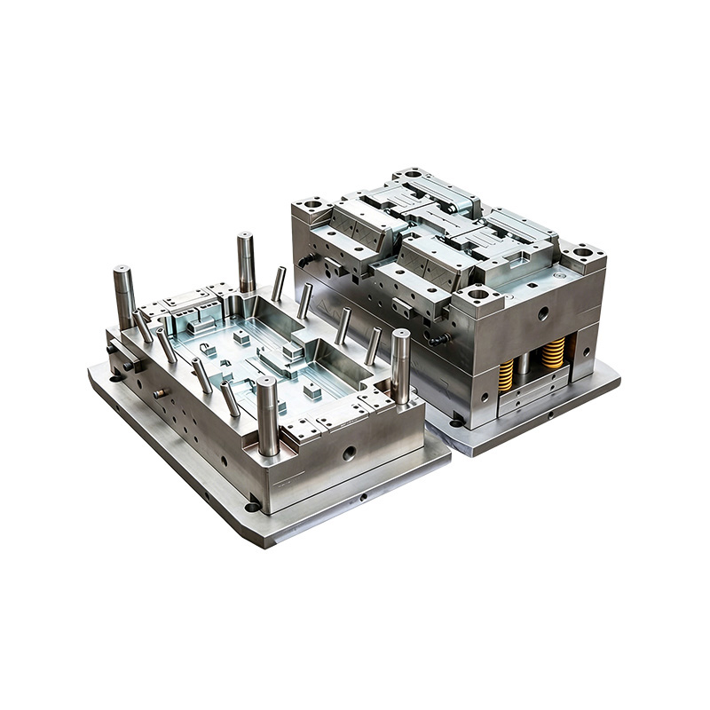
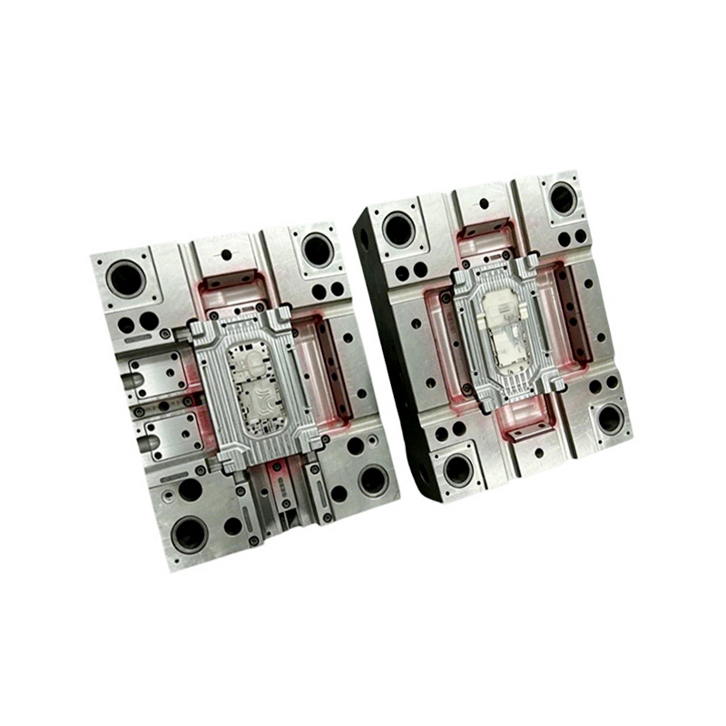
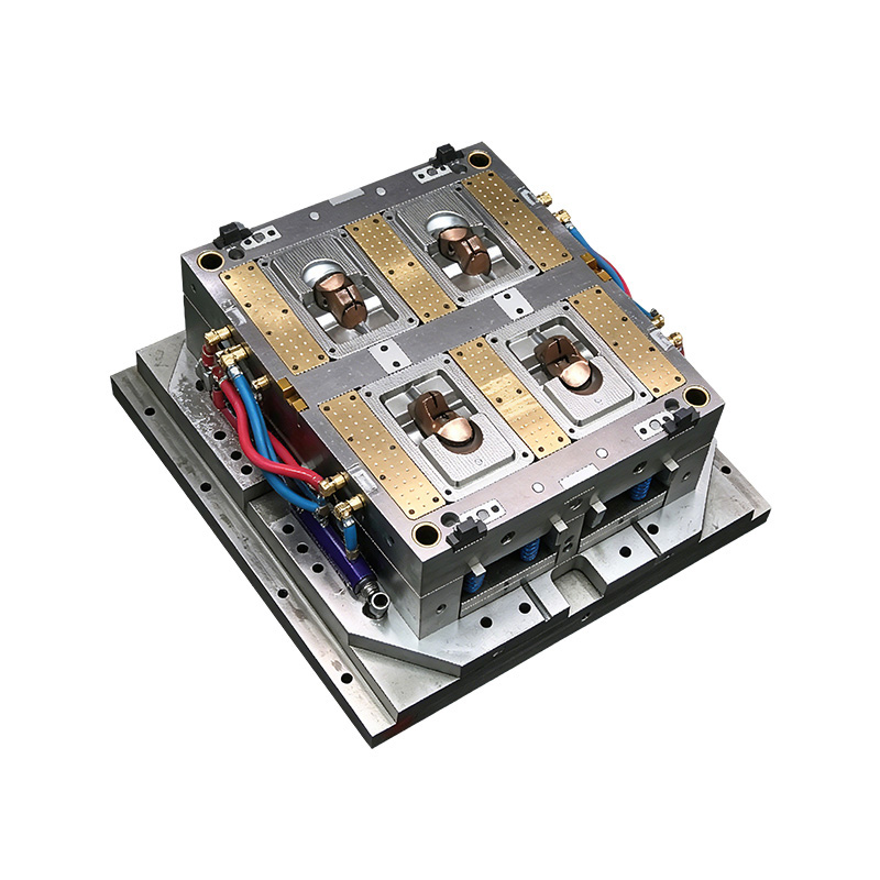
Electronic Precision Injection Molds are not simply tighter-tolerance versions of general-purpose tooling. They are designed from the start around the specific constraints of electronic component geometry: thin walls that must not warp, alignment features that locate PCBs or connectors with sub-millimetre precision, snap-fit hooks whose spring constant depends on exactly the right wall thickness and radius, and surface finishes that must meet cosmetic specifications or accept paint and plating adhesion without pre-treatment. Every element of the tool design — from gate type to parting line location to ejection method — directly affects the electronic component's final performance.
Mold Steel Expected Service Life by Grade (shots before cavity refurbishment, glass-filled resin)
Gate Selection for Electronics Molds
Gate type and placement in Electronic Precision Injection Molds must minimise gate vestige height, avoid weld lines across structural features, and provide balanced fill. The dominant gate choices:
Submarine (tunnel) gate: self-degates on ejection, zero operator intervention, vestige below part surface. Standard for high-volume precision consumer electronics housings.
Pin-point gate (3-plate): gate on top surface over the boss, degates automatically, gives central fill balance. Used for circular enclosures and switch housings.
Hot tip gate: no runner scrap, smallest vestige, best for cosmetic surfaces. Specified for premium consumer device enclosures and optical component bezels.
Edge (tab) gate: easy to adjust during development; used on prototype tools where vestige on a non-critical edge is acceptable.
Ejection Systems for Precision Electronics Parts
Ejection from an Electronic Precision Injection Mold must release the part without deforming thin walls, marking cosmetic surfaces, or stressing snap features. Ejection strategy options:
Ejector pin array: most common; pins positioned at thick sections away from cosmetic surfaces, sized to give even ejection force distribution.
Stripper plate: preferred for thin-wall cylindrical enclosures; the full plate pushes uniformly against the part's flange or rim.
Blade ejectors: used at ribs and thin vertical walls where a round pin would lack sufficient bearing area.
Air assist: used on very thin enclosures (wall below 0.8 mm) where any mechanical contact risks distortion.
Mold Venting: The Detail That Most Often Causes Surface Defects in Electronics Molds
As molten plastic fills an Electronic Precision Injection Mold cavity, the air inside must escape through vents machined into the parting line and around ejector pins. If air cannot escape fast enough, it is compressed ahead of the melt front and reaches temperatures above 300 degrees Celsius, burning the plastic and leaving a characteristic diesel burn mark at the last-to-fill point. Precision electronics molds use parting line vent depths of 0.010 to 0.020 mm for unfilled amorphous resins and 0.020 to 0.025 mm for glass-filled semi-crystalline resins, with the vent relief channel 0.5 to 1.0 mm deep. Vent cleaning is scheduled every 20,000 to 30,000 shots for glass-filled resins.
Scientific Injection Molding: The Process Methodology Behind Repeatable Precision
Scientific injection molding is the systematic application of rheological understanding and statistical process characterisation to establish a documented, robust molding process. It was developed and formalised by RJG Inc. in the 1990s and has since become the standard methodology for any injection molding program requiring Cpk greater than 1.33 on critical dimensions. The fundamental principle is that the molding process should be characterised by the plastic's actual state (melt viscosity, cavity pressure, melt temperature) rather than by machine set-point values, because machine set points are not directly transferable between different machines, while plastic state variables are material constants.
Scientific Injection Molding: 5-Step Process Characterisation Sequence
01
Viscosity Curve Study
The melt's apparent viscosity is measured across a range of injection speeds by recording the fill pressure at each speed for a short shot that fills to approximately 95 to 98% of cavity volume. Plotting fill pressure against injection rate produces the material's viscosity curve. The target injection speed is selected on the flat shear-thinning plateau region where viscosity is insensitive to small speed variations, making the process robust against machine-to-machine differences.
02
Gate Seal Study
The gate seal time is found by molding at progressively longer pack times and weighing each part. The part weight plateaus once the gate is sealed. All production shots use a pack time 10 to 20% longer than the measured seal time to ensure full packing regardless of minor viscosity variation between resin lots, eliminating sink marks and voids from under-packed parts.
03
Cooling Time Optimisation
Cooling time is established by incrementally reducing it and measuring part warpage and dimensional variation. The minimum cooling time that still produces parts within specification is selected. For scientific injection molding for electronics programs, the cooling time is validated by in-mold temperature measurement at multiple cavity locations to confirm consistent mold surface temperature before ejection on every cycle.
04
Process Window Definition and DOE
A factorial Design of Experiments varies the key process inputs at high and low levels and measures the effect of each variable on the critical output dimensions and cosmetic attributes. The DOE establishes which variables affect quality most and what their acceptable ranges are, producing the process window: a documented set of specification limits within which any combination of parameters produces conforming parts, independent of the specific machine used to run it.
05
Cavity Pressure Monitoring and Shot-by-Shot Control
In-cavity pressure sensors record the actual pressure profile inside the cavity on every shot. The peak cavity pressure and the cavity pressure integral are the most sensitive real-time indicators of whether a shot will be in tolerance. Control limits set on these sensor values allow the press controller to automatically reject shots that fall outside the validated process window, achieving zero-defect sorting without operator inspection of every part.
Process Capability (Cpk) Comparison: Scientific vs. Conventional Injection Molding on Critical Dimensions
Scientific Injection Molding for Electronics: Why Electronics Programs Need This Methodology
Scientific injection molding for electronics is not optional for programs producing connector housings, PCB frames, and fine-pitch electronic components. Consider a dual-row connector housing with pin pitch of 1.00 mm: the centre-to-centre distance between pin pockets must be held to ±0.02 mm across the full housing length to allow correct PCB foot pattern alignment. A connector housing 50 mm long must maintain dimensional control to 0.04 mm total variation across that span, achievable only with a fully characterised and cavity-pressure-controlled process. Specific benefits include process transferability across machines, systematic resin lot change management in 2 to 4 hours rather than days of trial and error, and the IQ/OQ/PQ validation documentation required by ISO 9001, IATF 16949, and ISO 13485 quality systems.
Precision Injection Molded Electronics Enclosures: Design, Features, and Industry Requirements
Precision injection molded electronics enclosures are the housings that protect, align, and present electronics assemblies in their final form. They range from palm-sized shells of consumer handheld devices to DIN-rail-mounted housings of industrial PLC modules and hermetically sealed enclosures of outdoor network equipment. The design requirements are substantially more demanding than for general plastic housings because the enclosure must simultaneously perform structural, cosmetic, electromagnetic, environmental sealing, and heat management functions — often within a total wall thickness of 1.2 to 2.5 mm.
Snap-Fit Engagement Force vs. Wall Thickness Variation (PC/ABS, 15mm cantilever arm)
EMC
EMI Shielding Integration
Precision injection molded electronics enclosures for wireless devices require electromagnetic interference (EMI) shielding through conductive coatings applied to the interior wall. The enclosure's dimensional precision determines how well the shielding layer contacts the PCB ground plane around the full housing perimeter. A gap of 0.3 mm or more in the shield contact interface can reduce shielding effectiveness by 10 to 20 dB at frequencies above 1 GHz.
IP
IP Sealing Interface Geometry
Gasket groove geometry for IP54 to IP68 rated enclosures must be held to tight tolerances. A groove 0.1 mm too wide allows the gasket to extrude under compression; a groove 0.1 mm too narrow prevents the lid from fully closing. Precision injection molding holds groove width to ±0.03 mm and groove depth to ±0.02 mm, reliably producing a seal interface within the gasket's specified compression range.
PCB
PCB Registration and Assembly
Boss centre-to-centre distances across a 120 mm wide enclosure must accumulate no more than ±0.15 mm total for screws to align with PCB holes on automated assembly lines. Precision injection molded electronics enclosures hold boss centre-to-centre distances to ±0.05 mm or better, providing a comfortable margin for automated PCB assembly.
UL
Flame Rating Compliance
Most electronics enclosure applications require UL 94 V-0 (self-extinguishes within 10 seconds, no dripping flaming material). The flame-retardant additives in V-0 grades affect resin viscosity, shrinkage, and surface finish. Precision molds for V-0 enclosures must be designed for the slightly different rheology of the FR-grade resin, and resin lot qualification must confirm that FR additive loading is within specification.
Frequently Asked Questions About Precision Injection Molding for Electronics
Q1What is precision injection molding and how is it different from standard molding?
What is precision injection molding? It is an injection molding approach in which tooling is machined to cavity tolerances of ±0.005 to ±0.010 mm, the process is characterised through systematic DOE testing, and critical process variables are controlled and monitored on every production shot. Standard molding accepts dimensional variation of ±0.1 to ±0.3 mm and relies on operator experience. Precision molding targets ±0.01 to ±0.05 mm and relies on documented process windows, in-cavity sensors, and statistical process control to maintain quality without operator intervention on every cycle.
Q2What makes Electronic Precision Injection Molds different from general tooling?
Electronic Precision Injection Molds differ in their steel specification (hardened to 48 to 52 HRC), their machining and polishing tolerances (cavity features held to ±0.005 mm, surface finish to Ra 0.02 micrometres for optical surfaces), their gate and runner design (minimising vestige height and weld line placement on functional surfaces), their cooling circuit design (maintaining cavity surface temperature uniformity within ±2 degrees Celsius), and their venting design (preventing burn marks at last-to-fill points without flashing). General tooling accepts wider tolerances because the parts produced do not require the dimensional and cosmetic consistency that electronic assembly demands.
Q3What is scientific injection molding and why does it matter for electronics?
Scientific injection molding is a process characterisation methodology that defines the molding process through the plastic's physical state (cavity pressure, melt viscosity, gate seal time) rather than machine set points. It matters for electronics because it produces a documented process window that can be transferred between machines, survives resin lot changes with systematic adjustment, and generates the validation documentation required by electronics OEM quality management systems. A program validated by scientific injection molding methodology typically achieves process capability (Cpk) above 1.67 on critical dimensions, compared to 0.8 to 1.2 for conventionally tuned programs.
Q4What tolerances can precision injection molded electronics enclosures hold?
Precision injection molded electronics enclosures produced with properly designed tooling and scientifically characterised processes routinely hold: overall external dimensions to ±0.05 mm on parts up to 200 mm; wall thickness to ±0.03 to ±0.05 mm; boss centre-to-centre distances to ±0.05 mm; snap-fit wall thickness to ±0.03 mm; and IP gasket groove geometry to ±0.02 mm on groove width and depth. For ultra-precision applications such as SMT connector housings in LCP, pin-to-pin pitch tolerances of ±0.01 mm are achievable.
Q5Which resins are best for precision injection molded electronics enclosures?
The best resin depends on application requirements. PC or PC/ABS blends are preferred for consumer device enclosures requiring good impact resistance, optical quality, and paintability, with shrinkage of 0.5 to 0.7% that is predictable and uniform. LCP is the choice for the tightest-tolerance connector housings, with shrinkage of only 0.1 to 0.3%, but it is expensive. PBT-GF30 is used for industrial and automotive electronics connectors where chemical resistance and low creep under fastener load are required, but its anisotropic shrinkage requires careful gate placement. ABS is the most economical option for enclosures without demanding thermal or chemical requirements.
Q6How does mold steel choice affect service life and surface quality of an electronics mold?
Mold steel choice is the single largest determinant of tool service life in Electronic Precision Injection Molds. P20 pre-hardened steel (300 to 330 HB) is fast to machine but wears significantly faster when running glass-filled resins. H13 hardened tool steel (48 to 52 HRC) resists abrasive wear and thermal fatigue, routinely reaching 500,000 to 1,000,000 shots before cavity refurbishment. S136 stainless (48 to 52 HRC) adds corrosion resistance for FR resins and is the standard for optical and mirror-finish enclosure cavities. NAK80 pre-hardened stainless (37 to 43 HRC) offers a compromise between machinability and polishability for mid-volume cosmetic enclosure programs.
Q7What is the role of cavity pressure sensors in scientific injection molding for electronics?
In-cavity pressure sensors are the most powerful tool in scientific injection molding for electronics because they measure the actual packing state of the plastic inside the mold on every single shot. The peak cavity pressure and pressure integral are set as control limits based on the validated process window. Any shot where cavity pressure falls outside these limits is automatically flagged and rejected before the part is ejected, providing 100% real-time sorting without human inspection. For electronics programs running at 500,000 to 2,000,000 parts per year, this automated sorting eliminates escape of out-of-tolerance parts to assembly and prevents field failures from dimensional non-conformance.
Q8How do warpage and shrinkage affect precision injection molded electronics enclosures?
Warpage occurs when differential cooling or differential shrinkage across the part creates internal stresses that cause the part to distort after ejection. For electronics enclosures, warpage manifests as a bow across a flat mating surface that prevents the seal groove from contacting the gasket uniformly, or that causes PCB boss heights to vary across the enclosure floor. Warpage is minimised through uniform wall thickness design (maximum wall-to-wall ratio of 1:1.25), balanced cooling in the mold, correct gate location, and selection of resins with low isotropic shrinkage. For flat precision injection molded electronics enclosures, warpage specifications are typically 0.2 mm maximum bow per 100 mm of length.
Q9What surface finishes are used on precision injection molded electronics enclosures?
Surface finishes are specified using SPI grades or VDI 3400 texture designations. SPI A1 and A2 (mirror polish with diamond compound) are used for optically clear lens windows. SPI B1 to B3 (600 to 400 grit paper finish) provide a matte sheen suitable for consumer device exteriors. VDI 3400 texture grades (VDI 12 to VDI 45) provide controlled matte to coarse textures for grip and paint adhesion. For enclosures that will be painted, a VDI 18 to VDI 24 texture is typical. The mold cavity must maintain its specified surface finish throughout the production run, requiring periodic re-polishing on a schedule determined by the abrasiveness of the resin.
Q10What documentation should a precision injection molding supplier provide for an electronics program?
A qualified supplier of Electronic Precision Injection Molds and scientific injection molding for electronics programs should provide: a mold design review package including mold flow simulation results; material certification and lot qualification records; First Article Inspection (FAI) reports with CMM measurement data for all critical dimensions in PPAP Level 3 format; viscosity curve, gate seal study, and DOE data from the scientific injection molding process characterisation; a documented process parameter sheet with all validated window limits; Cpk studies for a minimum of 30 production parts on every critical dimension; and a mold maintenance log template. This documentation package provides the evidence base required by ISO 9001, IATF 16949, and ISO 13485 quality management systems for supplier qualification and ongoing production monitoring.


 English
 Español

 View More
  View More
  View More






 Custom Precision Plastic Injection Mold Manufacturers